Video Article Open Access
Reverse Micelles as a Universal Route to Solution Processed Nanoparticles for Optical, Optoelectronic and Photonic Applications: A Story of Salt Complexation, Micellar Stability, and Nanoparticle Spatial Distribution
Ayse Turak
Department of Engineering Physics, McMaster University, Hamilton Ontario L8S 4L7, Canada
Vid. Proc. Adv. Mater., Volume 2, Article ID 202103166 (2021)
DOI: 10.5185/vpoam.2021.03166
Publication Date (Web): 27 Jul 2021
Copyright © IAAM
Graphical Abstract
Abstract
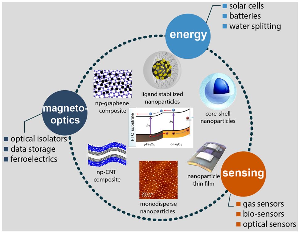
Over the past two decades, nanometer-sized materials and devices have attracted much interest from scientists and the general public, due to the broad range of current and prospective applications of nanomaterials in electronics, high-density data storage, chemical sensing, drug delivery, medical diagnostic systems, and nanocatalysis. The explosive growth in solution processed semiconductors has driven new emerging technologies for photonic sources and adaptive optics: organic, hybrid, perovskite and all inorganic-nanoparticle systems have developed significantly over the last four decades due to the promise of cheap, flexible displays and lights and the sources to power them. Though they have impacted the consumer landscape, such devices have not dominated the market as has been long predicted, as a roadblock in effective nanoparticle device development is homogeneity, uniformity and effective size control, in the materials and at various interfaces. Self-assembly of amphiphilic block copolymers is a model example of a "bottom-up" approach to the construction of nano-objects on large areas. Di-block copolymers, due to their amphiphilic nature, spontaneously form core-corona micelles in selective solvents. Using the micelles as “nanoreactors” allows the formation of highly controllable nanoparticles. Particles are possible with a very narrow size distribution, less than 2% variation in the particle diameters, which can be deposited on any surface at room temperature with highly controlled spacing and spatial organization. This is a simple manufacturing approach, that is low-cost, low-energy, and can be scaled-up to industrial scales. An advantage of the reverse micelle approach is the control over the 2D dispersion: highly ordered periodic arrays to complete spatial randomness are achieved with simple tuning of deposition parameters. In the Organic Interfaces Group at McMaster University, we have used the same basic micellar diblock copolymer nanoreactor to produce monodisperse oxide, dielectric, perovskite, and metal nanoparticles [1–5] for use as electrode interlayers in optoelectronic devices, as catalysts for water splitting, as optical isolators, and as nanoparticle polarizers. Most recently, we have expanded the approach to produce highly luminescent monodispersed organo-halide perovskite nanoparticles for light emitting diodes and lasers. This talk will cover our recent developments in reverse micelle deposition of ordered arrays of functional nanoparticles and their impact on various devices. Taking advantage of the tunability of these templates, we are able to produce particles of varying composition, structure, and size to achieve tunable magnetic, electrical, and optical responses. As it can be difficult to classify disordered systems, we have also developed a variety of tools to quantify the spatial order of nanoparticles, collected in a freely available Mathematica package, “Detecting Intermolecular Structure Located at particle positions” (dis-Locate). With a complete picture of the synthesis process coming out of our research -- from an understanding of the basic loading behaviour, the stability and the organizational structure of the micelles, to the properties of the nanoparticles and their impact in devices -- it is possible to tailor nanoparticle properties for widespread applications. This universal low-cost facile route to monodisperse single phase nanoparticles offers a roadmap for further developments of functional nanoparticles tailored for bespoke applications.
Keywords
Reverse micelle deposition, diblock copolymer lithography, complexation, nanoparticle synthesis, organic electronics.
Acknowledgement
This work was supported by Ontario Ministry of Research and Innovation Early Researcher Award (ER15-11-123), the Natural Science and Engineering Council of Canada (RGPIN-2019-05994), Satellite Canada Innovation Network (HTSN-611).
References
- K. Liang, L. Shu Hui, A. Turak, Nanoscale 2019, 11, 9076.
- L. S. Hui, C. Beswick, A. Getachew, H. Heilbrunner, K. Liang, G. Hanta, R. Arbi, M. Munir, H. Dawood, N. Isik Goktas, R. R. LaPierre, M. C. Scharber, N. S. Sariciftci, A. Turak, ACS Appl. Nano Mater. 2019, 2, 4121.
- S. I. Lee, G. J. Yun, J. W. Kim, G. Hanta, K. Liang, L. Kojvic, L. S. Hui, A. Turak, W. Y. Kim, Scientific Reports 2019, 9, 2411.
- S. I. Lee, K. Liang, L. S. Hui, R. Arbi, M. Munir, S. J. Lee, J. W. Kim, K. J. Kim, W. Y. Kim, A. Turak, J Mater Sci: Mater Electron 2021, DOI 10.1007/s10854-020-04889-0.
- T. Tokubuchi, R. I. Arbi, P. Zhenhua, K. Katayama, A. Turak, W. Y. Sohn, J. Photochem. Photobiol. A 2021, 410, 113179.
Biography
Ayse Turak is an Associate Professor in the Department of Engineering Physics at McMaster University. Her research focusses on growth of organic and hybrid organic-inorganic (perovskite) thin films and nanoparticles for microelectronics. Her vision is to develop easy, versatile, and inexpensive methods of exploring and tuning interfaces, particularly in organic and hybrid solar cells, light emitting diodes and sensors. By making electronic products cheaper, more accessible, and more flexible, her research will have a huge impact on the way people use clean energy, access information and measure the world around them. To achieve this vision, the Turak group uses simple manufacturing approaches (reverse micelle deposition), allows nature to dictate morphology (entropic self-assembly, beneficial dewetting), and develops widely applicable characterization tools (“MORPHOLOGIES” Monte Carlo simulation code, “dis-Locate” spatial order classification package, 3D printed environmental testing chamber). Her main research thrusts are the facile growth of functional nanoparticles, spatial order in nanoparticles for interfacial tuning, and tools to control degradation at interfaces. Dr. Turak is an expert in materials and surface science, with 15 years of experience in the growth of nanoparticles and organic films. Prior to McMaster, she was a Marie Curie Fellow at the Max-Planck-Institute for Metals Research in Stuttgart, Germany (2008-2010), then a visiting professor at Sabanci University in Istanbul, Turkey (2011). She has received an Early Researcher Award (2016), a Leadership in Teaching and Learning Fellowship (2017-2019) and the Petro-Canada Young Innovators award (2016). She is currently the co-chair for the Canadian chapter for the Society for Information Display, and on the Editorial Board for the Journal of Materials Science: Materials in Electronics (Springer) and Scientific Reports (Springer-Nature), and Associate editor for Frontiers in Photonics in Photovoltaic Materials and Devices. She is a member of the intelliFLEX Innovation Alliance, and a member of EVATEG (Energy Efficient Electronic and Lighting Technologies Research Centre, Turkey).
Video Proceedings of Advanced Materials
Upcoming Congress
