Video Article Open Access
Light for Hydrogen: Nanostructure Design for Solar Water Splitting
Francesco Caddeo, Behzad Mahmoudi, Florian Himmelstein, Denis Eberhart, Titus Lindenberg, Haojie Zhang, Robert Naumann, A. Wouter Maijenburg*
Center for Innovation Competence SiLi-Nano, Martin-Luther-University Halle-Wittenberg, Halle (Saale), 06120, Germany
Vid. Proc. Adv. Mater., Volume 2, Article ID 2021-03163 (2021)
DOI: 10.5185/vpoam.2021.03163
Publication Date (Web): 08 May 2021
Copyright © IAAM
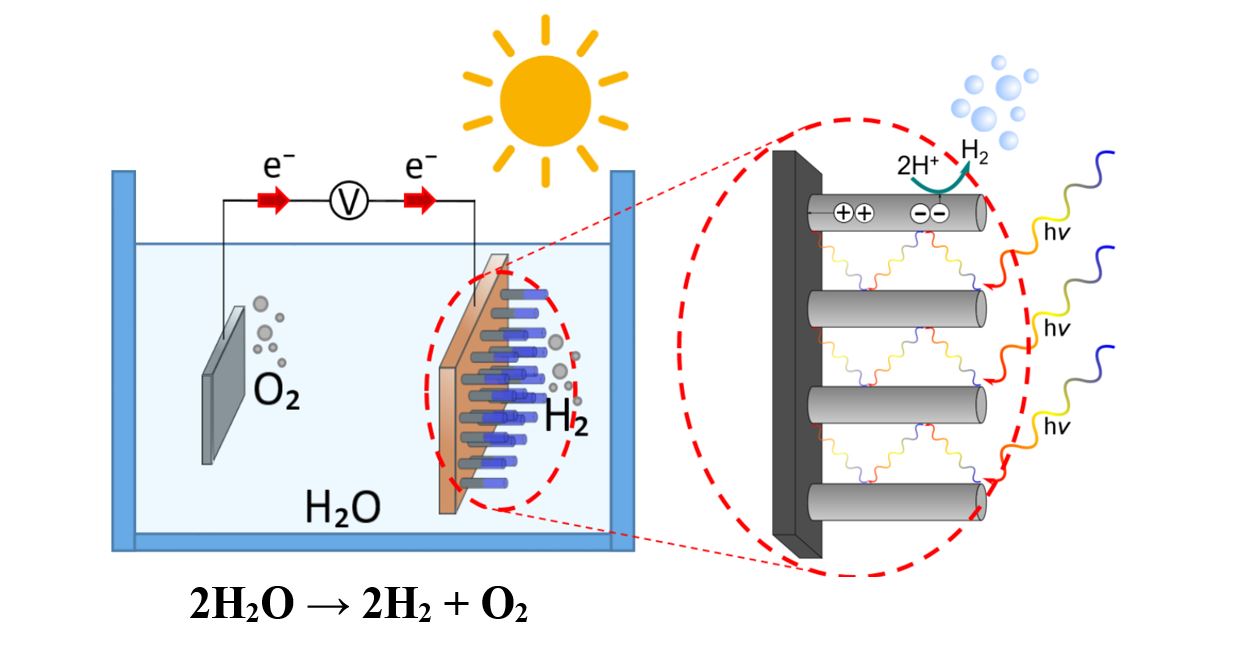
Graphical Abstract
Abstract
The unique physical and chemical properties of quasi one-dimensional nanostructures that arise by their high surface-to-volume ratio make these nanostructures very promising for many applications, including solar water splitting. Furthermore, the physical properties of most semiconductors also demand the use of such elongated nanostructures for photo(electro)chemical applications. For instance, the diffusion length of minority charge carriers (i.e., electrons for a p-type semiconductor or holes for an n-type semiconductor) in Cu2O is only 20-100 nm, while the absorption depth near the bandgap is approximately 10 µm. This means, that with the use of one-dimensional nanostructures, a maximum of solar light can be absorbed over the nanowire length, while the nanowire diameter is small enough for efficient electron and hole diffusion, and therefore high efficiency. This concept forms the basis of the research that is performed within my group. In the past, we for instance successfully developed ZnO and Cu2O nanowires and nanowire networks that presented a significantly improved PEC performance when compared to their thin film counterparts [1,2]. And currently, we are for instance focused on the development of core-shell Cu2O@MOF nanowires, CuBi2O4 nanowires and nanofibers via templated electrodeposition and electrospinning, respectively, and we are also investigating the use of the more traditional PV-materials Si and CuGaSe2/CuGa3Se5 for photoelectrochemical water splitting.
Within this presentation, I will focus on two of our recent achievements, namely (i) the synthesis of core-shell Cu2O@MOF nanowires and (ii) the successful application of CuGaSe2/CuGa3Se5 films for photoelectrochemical water splitting.
For the preparation of the core-shell Cu2O@MOF nanowires, we combined two established synthesis techniques, where we first used templated electrodeposition for the preparation of supported, open-porous and well-defined Cu2O nanowire networks, which were subsequently converted into a MOF (e.g., Cu3(BTC)2) via electrochemical oxidation inside an electrolyte containing the respective organic linkers. Herein, the large flexibility of both techniques can be used to fine-tune the dimensions of the obtained Cu2O nanowires and the surrounding nanoMOF crystals, as well as the chemical functionality of the nanoMOFs. Additionally, we were also able to obtain nanowires that completely consist of a Cu-based MOF [3].
In a different project, we prepared polycrystalline Cu-Ga-Se films with different compositions ranging from Cu-poor CuGaSe2 (Cu/Ga = 0.85) to extremely Cu-poor CuGa3Se5 (Cu/Ga = 0.33) and investigated the effect of the Cu/Ga ratio on the crystal structure, morphology and PEC performance of the films. Without any surface treatment or formation of a p-n junction, we obtained remarkable saturated photocurrent densities of -19.0 and -12.1 mA/cm2 (measured at -0.40 V vs. RHE) for our films with Cu/Ga = 0.85 and Cu/Ga = 0.33, respectively, using an LED-based solar simulator. These outstanding results cover 86% and 68% of the maximum theoretical photocurrents for materials with a band gap of 1.68 eV and 1.85 eV, respectively [4].
Keywords
(Photo)electrochemistry, water splitting, Metal-Organic Frameworks, nanoMOFs, CuGaSe2/CuGa3Se5
Acknowledgement
Financial support from the Bundesministerium für Bildung und Forschung (BMBF; grant no. FKZ:03Z22HN11) is greatly acknowledged.
References
- L. Movsesyan, A.W. Maijenburg, N. Goethals, W. Sigle, A. Spende, F. Yang, B. Kaiser, W. Jaegermann, S.Y. Park, G. Mul, C. Trautmann and M.E. Toimil-Molares, Nanomaterials, 2018, 8, 693.
- F. Yang, C. Schröck, J. Kugelstadt, S. Zhang, C. Scheu, C. Trautmann, A.W. Maijenburg and M.E. Toimil-Molares, Zeitschrift für Physikalische Chemie, 2020, 234, 1205.
- F. Caddeo, R. Vogt, D. Weil, W. Sigle, M.E. Toimil-Molares and A.W. Maijenburg, ACS Applied Materials & Interfaces, 2019, 11, 25378.
- B. Mahmoudi, F. Caddeo, T. Lindenberg, T. Schneider, R. Scheer and A.W. Maijenburg, Manuscript under revision for publication in Electrochimica Acta.
Biography
A. Wouter Maijenburg obtained his PhD degree from the University of Twente (Enschede, The Netherlands) in 2014. During his doctorate studies, he performed 4 months of his PhD research at Purdue University (West Lafayette, Indiana, USA) in the fall of 2011, for which he obtained a Fulbright Visiting Scholar scholarship. Additionally, in 2012 he was the chair of the first Gordon Research Seminar (GRS) on Electrodeposition. After his PhD, he obtained a Humboldt Fellowship for Postdoctoral Researchers, which he used for performing 2 years of postdoctoral research at the GSI Helmholtz Centre for Heavy Ion Research (Darmstadt, Germany).
In October 2016, he became a Junior Professor at the Martin-Luther-University Halle-Wittenberg, where he holds the chair of Inorganic Functional Materials within the Institute of Chemistry, and he is the leader of the Light for Hydrogen group within the Centre for Innovation Competence (ZIK) SiLi-nano. Additionally, since January 2020 he is a member of the external advisory board for the Neo-PEC project of the Fraunhofer Institutes CSP, IST and IKTS.
Wouter Maijenburg’s research is mainly focused on the nanostructure design for solar water splitting, for which his group is currently investigating several different synthesis procedures (e.g., templated electrodeposition, anodization, electrospinning, co-evaporation and atomic layer deposition) in order to obtain optimized nanostructures of several different materials (e.g., Metal-Organic Frameworks (MOFs), Cu2O, CuBi2O4, BiVO4, Si, CuGaSe2/CuGa3Se5 and CoP). In addition to the standard characterization methods, his group is also using techniques like femtosecond transient absorption spectroscopy (fs-TAS) in order to understand the physical phenomena that take place in their semiconductor materials and nanostructures.
Video Proceedings of Advanced Materials
Upcoming Congress
