Video Article Open Access
2D Straintronic Devices
Patricia Gant1, Qinghua Zhao1,2,3, Yu Kyoung Ryu1, Felix Carrascoso1, Hao Li1, Tao Wang2,3, Peng Huang1,4, David Pérez de Lara5, Dan Guo4, Riccardo Frisenda1, Andres Castellanos-Gomez1,*
1Materials Science Factory, Instituto de Ciencia de Materiales de Madrid (ICMM-CSIC), Madrid E-28049, Spain
2State Key Laboratory of Solidification Processing, Northwestern Polytechnical University, Xi'an, 710072 P. R. China
3Key Laboratory of Radiation Detection Materials and Devices, Ministry of Industry and Information Technology, Xi'an, 710072 P. R. China
4State Key Laboratory of Tribology, Tsinghua University, Beijing 100084, China
5Guangdong Technion - Israel Institute of Technology Shantou, China
Vid. Proc. Adv. Mater., Volume 2, Article ID 2021-0191 (2021)
DOI: 10.5185/vpoam.2021.0191
Publication Date (Web): 20 Mar 2021
Copyright © IAAM
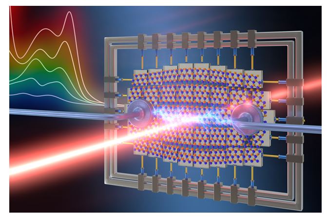
Graphical Abstract
Abstract
Strain engineering is an interesting strategy to tune a material’s electronic properties by subjecting its lattice to a mechanical deformation. Conventional straining approaches, used for 3D materials (including epitaxial growth on a substrate with a lattice parameter mis-match, the use of a dielectric capping layer or heavy ions implantation) are typically limited to strains lower than 2% in most cases due to the low maximum strains sustained by brittle bulk semiconducting materials. Bulk silicon, for example, can be strained only up to 1.5% before breaking. Moreover, these straining approaches induce static deformations of the semiconductor materials and therefore they are not suitable for tunable functional devices. 2D materials, on the other hand, can be literally stretched, folded, bent or even pierced standing remarkably large deformation before rupture [1]. This outstanding stretchability (and the possibility of using dynamically varying strain) of 2D materials promises to revolutionize the field of strain engineering and could lead to "straintronic" devices – devices with electronic and optical properties that are engineered through the introduction of mechanical deformations. In this talk I will discuss our recent efforts to study strain engineering in 2D materials and to exploit it to fabricate strain tunable functional optoelectronic devices [2-7].
Keywords
Straintronics; strain engineering; optoelectronics; molybdenum disulfide (MoS2); 2D materials.
Acknowledgement
This project has received funding from the European Research Council (ERC) under the European Union's Horizon 2020 research and innovation programme (grant agreement n° 755655, ERC-StG 2017 project 2D-TOPSENSE) and the European Union’s Horizon 2020 research and innovation program under the Graphene Flagship (grant agreement number 785219, GrapheneCore2 project and grant agreement number 881603, GrapheneCore3 project).
References
- R Roldán et al. Journal of Physics: Condensed Matter 2015, 27 (31), 313201.
- R Frisenda, et al. npj 2D Materials and Applications 2017, 1 (1), 10.
- P Gant, et al. Materials Today 2019, 27, 8-13.
- YK Ryu, et al. Nano Letters 2020.
- F Carrascoso, H Li, et al. Nano Research 2020.
Biography
Andres Castellanos-Gomez is a Tenured Scientist in the Spanish National Research Council (Consejo Superior de Investigaciones Científicas, CSIC). He graduated in Physics in the Universidad Complutense of Madrid (Spain) in 2006 and got his PhD by the Autonoma University of Madrid (Spain) with Cum-Laude and Extraordinary Award. From 2011 till 2015 he was a post-doctoral researcher at the Kavli Institute of Nanoscience in the group of Prof. van der Zant where he got a Marie Curie Fellowship. In 2015 he got a Tenure Track position at the IMDEA Nanoscience Research Institute of Madrid and in 2017 he got his actual Tenured Scientist position at CSIC. He explores novel 2D materials and studies their mechanical, electrical and optical properties with special interest on the application of these materials in nanomechanical and optoelectronic devices. He authored ~140 articles in international peer review journals and 6 book chapters. According to Google Scholar, A. Castellanos-Gomez has an h-index of 50, with a total number of citations above 13,000. He was awarded an ERC Starting Grant in 2017 and has been selected as Emerging Leader 2020 by Journal of Physics: Materials, included in the Highly Cited Researchers 2018 and 2019 lists of Clarivate/WOS, selected as one of the 2018 Emerging Investigators by Chemical Society Reviews and selected as one of the Top Ten Spanish Talents of 2017 by the MIT Technology Reviews. He has been also recognized with the Young Researcher Award (experimental physics) of the Royal Physical Society of Spain (2016).
Video Proceedings of Advanced Materials

Upcoming Congress
