Video Article Open Access
Materials and Device Design for Thin-film intermediate band solar cells
Nazmul Ahsan1,*, Yoshitaka Okada1,2
1Research Center for Advanced Science and Technology, University of Tokyo, Tokyo, 153-8904, Japan
2Department of Electrical and Electronic Engineering, University of Tokyo, Tokyo, 113-8656, Japan
Vid. Proc. Adv. Mater., Volume 2, Article ID 2021-0162 (2021)
DOI: 10.5185/vpoam.2021.0162
Publication Date (Web): 09 Feb 2021
Copyright © IAAM
Graphical Abstract
Abstract
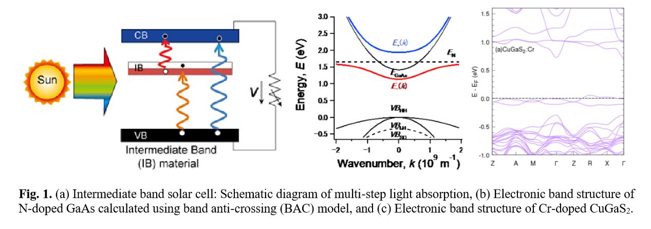
Intermediate band solar cells (IBSCs) are expected to exceed the theoretical conversion efficiency of single junction solar cells [1] due to the build-up of long-wavelength photocurrent assisted by two-step photon absorption (TSPA). However, the TSPA in experiments of below-bandgap solar radiation has been too weak producing only small photocurrent increments in present materials including III-V quantum dots [1] and III-V dilute nitrides [2].
The key materials parameters to improve the IBSC performances are: (1) a reasonably wide-bandgap semiconductor material that can reduce the loss of hot-electron energies produced by the short-wavelength solar spectrum photons, and (2) a suitable intermediate band (IB) or states existing roughly around the position of 1/3 or 2/3 of the bandgap that can increase the short circuit current, ISC, by absorbing long-wavelength solar photons. In order for an efficient TSPA production, it is required that the Fermi level EF stays inside the IBs. On the other hand, the key device requirement is the perfect electrical isolation of the IB from the metal contacts which only allows the selective collection of photo-carriers from the band edges. The design of a suitable energy barrier layer can realize the electrical isolation by blocking the escape pathways of the IB electrons to the contacts.
In this talk, we focus on two compound semiconductor systems, promising for high efficiency IBSC application, based on calculation and experiments: III-V GaAs-base dilute nitrides [2], and I-III-VI2 CuGaS2-based chalcopyrite sulphides [3]. In the prior, the splitting of the conduction band (CB) into two sub-bands makes them promise for IBSC application, and the magnitude of bandgap between them can be artificially designed by the amount of nitrogen. In the latter, deep impurity states are promoted into intermediate bands by raising the concentration above Mott transition level inside a wide bandgap CuGaS2 host. We discuss about the device design and characteristics of the respective systems, and their future outlook.
Keywords
Intermediate band solar cells, III-V dilute nitride and chalcopyrite semiconductors, density functional theory.
Acknowledgement
This work is supported by New Energy and Industrial Technology Development Organization (NEDO), and Ministry of Economy, Trade and Industry (METI), Japan, and by JSPS KAKENHI Grant Number 18K04224.
References
- Y. Okada, et al., Applied Physics Reviews, 2015, 2, 021302.
- Ahsan, et al. Appl. Phys. Lett., 2012, 100, 172111.
- N. Ahsan, et al., Proc. PVSC, 2017, 667.
Biography
Nazmul Ahsan received the M.S. and Ph.D. degrees in electronic engineering from The University of Tokyo, Japan, in 1999 and 2002, respectively. He is currently a Research Associate Professor at the Research Center for Advanced Science and Technology (RCAST) at the University of Tokyo. His research interests include ultra-high-efficiency photovoltaic devices, spintronic devices, Molecular Beam Epitaxy of compound semiconductors, Materials design and characterization. Dr. Ahsan is a member of IEEE, Japan Society of Applied Physics (JSAP), and American Physical Society (APS). He has been serving as the PI and Co-PI of several government and international funded projects and published around 100 scientific articles.
Video Proceedings of Advanced Materials
Upcoming Congress
